A well-structured, efficient product development process is the difference between market leadership and missed opportunity in the demanding world of electronic hardware. It ensures products not only meet rigorous technical specifications, exceed user expectations, accelerate time-to-market, control costs and reduce risks at every stage of the development cycle.
By aligning cross-functional teams, streamlining workflows, and fostering seamless communication, a robust process significantly enhances the ability to compete, adapt, and succeed in today’s fast-moving, fiercely competitive electronics market. It must remain agile - ready to respond to shifting strategies, evolving customer needs, emerging technologies and new market trends. That’s why our approach is built on flexibility from the ground up, ensuring readiness for future challenges. On this page, we’ll walk you through the key steps that take your new product from concept to launch.
Before we begin the development process, working closely with stakeholders, it's essential to first identify your direct competitors and gather product ideas. This involves researching similar products to understand what other companies are offering.
Equally important is gaining deeper insight into the market and identifying the needs of potential users. If there's a specific problem or missing feature that hasn't been addressed yet, this presents an opportunity to create a targeted solution that fills that gap.
Through comprehensive market research, we can define a realistic budget, set clear business objectives, and outline the right development strategy for your product.
The Product Definition Phase focuses on planning the product’s features, functionality and electronic components. Depending on the complexity, this phase can take anywhere from a few weeks to several months. It typically includes the following steps:
█ Brainstorming ideas.
█ Carrying out site visits.
█ Creating a product concept.
█ Drawing up a preliminary project.
█ Plan and prioritize tasks.
A preliminary product design is essential for effectively managing the development project. This phase covers both the electronic and mechanical components of the product, along with defining requirements, specifications, estimated costs, profit margins, and a feasibility analysis. It provides a clearer understanding of the product’s potential and helps evaluate its overall profitability.
The system-level block diagram is a critical tool in the preliminary design phase, providing a high-level visual representation of the interconnections between functional components. Most embedded systems incorporate microprocessors or microcontrollers interfacing with various active (e.g., sensors, ICs) and passive (e.g., switches, motors) components. Defining this architecture enables us to identify all necessary subsystems, communication protocols, and power requirements, allowing for the selection of appropriate processing units and peripheral interfaces tailored to the product’s functional specifications.
At the next stage, we identify and evaluate manufacturers and suppliers capable of providing the required components and semi-finished products necessary for the new design. We compile a comprehensive list of all fundamental components to generate a preliminary Bill of Materials (BOM). The BOM outlines each part, its specifications, unit cost, and sourcing options, serving as a foundational document for both prototyping and mass production. This component overview is essential for accurately estimating production costs and planning the financial aspects of the overall product development lifecycle.
When evaluating the cost and feasibility of a product or project, relying solely on the Bill of Materials (BOM) provides only a partial view of the overall cost structure. While the BOM outlines direct component costs, it does not capture the full range of factors that influence the total development and industrialisation cost required to bring a product to production readiness.
To enable accurate budgeting in later stages of development, as well as effective strategic planning and informed decision-making, a holistic approach to cost assessment is essential. During the early development phase, cost estimates are typically indicative and based on limited data. However, as the concept matures, a more precise and comprehensive cost model becomes critical to validate feasibility and align cross-functional expectations.
This refined analysis involves evaluating the broader cost structure behind a manufactured product. In addition to assessing the Cost of Goods Sold (COGS) and Total Cost of Ownership (TCO), it incorporates a pre-validated should-cost analysis (SCA) - an upfront assessment used to define a realistic and justifiable manufacturing cost before procurement evaluates supplier pricing. Together, these frameworks help uncover hidden cost drivers and identify opportunities for efficiency and value optimisation across the supply chain.
By integrating these methodologies and enhancing them with AI-driven tools, we can identify and manage a broader range of cost drivers, including but not limited to:
█ Direct material costs (BOM):
● Raw materials (e.g., PCBs, semiconductors, batteries)
● PCB fabrication and assembly
● Enclosure manufacturing (e.g., injection molding, CNC machining)
● Wiring, connectors, and cable harnesses
● Standard product packaging materials
● Fasteners, adhesives, coatings and consumables
█ Direct labor costs:
● Manual assembly labour
● Supervision in automated production lines
● Wages, benefits and payroll-related costs for production personnel
█ Manufacturing overhead (apportioned to production):
● Factory utilities (electricity, water, etc.)
● Depreciation of manufacturing equipment
● Factory rent or lease costs
● Maintenance and repair of production equipment
● Factory consumables (e.g. lubricants, cleaning materials)
█ Production-specific costs:
● Tooling and setup costs (amortised across production volumes)
● Testing and quality control (unit-level or batch-level testing)
● Subcontracted or outsourced manufacturing services
█ Inbound logistics:
● Freight-in (transport of materials and components to the production facility)
● Customs duties and import fees
█ Other direct production costs:
● Product-specific packaging assembly (e.g., custom-fit foam, internal trays)
● Scrap and production waste (where structurally expected and accounted for)
By integrating Artificial Intelligence (AI) across the entire product lifecycle (from initial concept to detailed, data-driven cost models) we can eliminate unforeseen cost overruns and reduce financial risk. AI-driven simulations and predictive analytics provide real-time insights into material choices, manufacturing processes, supply chain dynamics, and operational constraints, enabling accurate cost breakdowns early in development.
Within our Ultimate Development Roadmap, AI is embedded at key milestones: ideation, design, validation, sourcing and production, creating a cohesive, data-informed framework that aligns with product goals, team workflows and business objectives.
This integration enhances COGS, TCO, and pre-screened Should-Cost Analysis, making them not only more precise but also adaptable to design changes, market shifts and supplier performance variations. The result is a technology-driven approach that transforms cost modelling into a strategic tool; supporting faster decisions, optimized resources and strong cross-functional alignment.
The Architecture phase is focused on defining the product’s foundational structure. This involves identifying key system components, their interactions and the principles guiding the product’s technical direction. Decisions about technology stack, data flows, scalability and security are made here to ensure the product can be built on a robust and sustainable foundation.
Once the high-level architecture is outlined, a Proof of Concept (PoC) may be developed to validate these assumptions in practice. A PoC is a simplified prototype that tests the core architectural choices and demonstrates that the underlying concept is technically viable. While it does not reflect the final product design, it provides early insights and feedback, ensuring that critical risks are addressed before investing heavily in full-scale development.
Together, architecture and PoC help establish both the structural blueprint and the practical feasibility of the product, aligning vision with reality and reducing risk before moving forward.
The design of the electronic hardware is carried out using Altium™ Designer, a professional PCB design software suite.
At this stage, we focus on developing two key components:
█ Schematic Circuit Diagram.
█ Printed Circuit Board (PCB).
The Schematic Circuit Diagram is an advanced and detailed representation of the initial system block diagram created in the early stages of the project. At this point, each block is expanded to include all relevant sub-circuits, resulting in a complete schematic of the electronic system. It is important to note that this is not a basic or conceptual diagram, it must comprehensively include every component required in the final product. Any misplacement or incorrect implementation of a part can significantly impact the device’s performance and functionality.
Once the schematic is finalized, we proceed to design the Printed Circuit Board (PCB). The PCB is the physical foundation of the electronic product, a fiberglass board with copper traces that electrically connect all components. Depending on complexity, some PCBs require multi-layer technology, using several copper layers to accommodate high-density designs.
Altium™ Designer provides integrated validation tools to verify the PCB layout and ensure compliance with design specifications. It's critical that the PCB meets all quality and design standards to guarantee proper functionality.
The time needed to complete the PCB layout varies based on the board’s size, complexity and the specific design requirements. Special attention must be given to voltage routing, RF clock signals, high-speed data paths, wireless circuit design, current flow optimization and grounding strategies to ensure optimal performance and stability.
Manufacturing the first version of a PCB doesn’t guarantee flawless operation. Before moving forward with a fully functional prototype (commonly referred to as Proto-0), the board must undergo thorough testing to identify and resolve any
bugs
Origin of the term “bug”
The term “bug” was popularized in 1947 when engineers working on the
Harvard Mark II electromechanical computer discovered a moth trapped
in relay panel “F”, causing a malfunction. The incident was recorded
as the first actual case of a bug being found.
The word had already been used earlier by inventor Thomas Edison in
the 1870s to describe technical faults in electrical inventions. The
1947 event helped establish its modern meaning in electronics and
computing: a fault, glitch, or unexpected behavior in hardware or
software systems.
or performance issues.
At this stage, it’s common to encounter software-related problems involving the microcontroller or embedded processor. The Microcontroller Unit (MCU) - often working alongside or integrating the processor core - acts as the device’s “digital traffic controller,” orchestrating interactions between key components such as memory, sensors, actuators, displays and switches. When issues arise within the firmware running on the MCU, it typically requires reprogramming or further debugging.
To develop and debug embedded code, our engineers use Visual Studio Code together with toolchains and compilers for languages such as C and C++. For specialized embedded-audio environments, we alternatively use CodeFusion Studio™ from Analog Devices™, a dedicated toolchain designed specifically for their DSP and audio-processing platforms. The development process involves iterative cycles of debugging, testing and evaluating changes - this cycle is repeated as needed - until not only the correct system behavior is accomplished, but also stable and reliable operation.
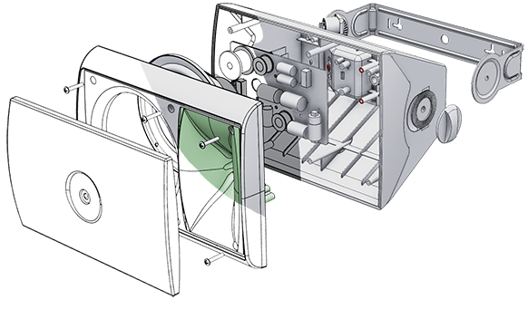
The PCB prototype has been successfully developed and tested. The next crucial step is integrating all components to better visualize the final product’s appearance and functionality.
The steps for creating a prototype its Physical Design include:
█ Designing a 3D model.
█ Building the 3D prototype.
█ Evaluating the prototype.
Before creating the actual physical prototype, it's essential to first visualize the product. This involves collaborating with a 3D Modeler or Industrial Designer to create a detailed 3D model using software like SolidWorks™ or AutoDesk™ 3ds Max.
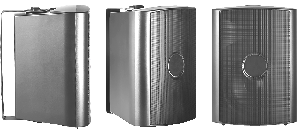
Once the digital 3D model is complete, it can serve as a powerful marketing tool, helping customers understand what the product will look like. Alternatively, you may choose to skip this step and proceed directly to building the physical prototype.
To construct a physical 3D prototype, an additive manufacturing process, commonly known as 3D printing, is used. This process builds the object layer by layer using plastic. However, it's important to note that the resin used in 3D printing differs in both appearance and properties from the plastics used in Micro Injection Molding (MIM). MIM allows for much smoother surfaces and significantly tighter tolerances (ranging from 10 to 100 microns) than typical 3D printing.
After producing the initial prototype, it’s common to identify areas that need refinement. Before conducting any formal testing, we recommend producing multiple versions of the prototype. This enables a thorough and accurate evaluation, ensuring that the final, market-ready electronic product meets all design and functionality expectations. Iteration during this phase is often necessary to achieve the desired outcome in terms of aesthetics, usability and performance.
With the prototype now developed, the next step, before drafting a full Production Manual and entering mass production, is to begin creating Pilot units.
Pilots are the first hardware units manufactured during the product development cycle. These early versions are designed and built by our team based on the feedback and adjustments identified during the prototype evaluation phase. The purpose of Pilot units is to collect real-world feedback from end users, identify any remaining issues and assess potential risks before committing to large-scale manufacturing.
Following the pilot phase comes the full production stage, where manufacturers begin large-scale fabrication of the electronic hardware for customer delivery. During this stage, Quality Control Managers and Supervisors carry out detailed inspections of processes and components, both individual parts and semi-finished assemblies, to fine-tune the production workflow and ensure the highest product quality.
Developing Pro Audio products is a complex, multi-layered endeavor that goes far beyond what we can cover here. From high-performance AD/DA conversion, embedded systems, and analog/digital circuit design to advanced DSP processing techniques for mixing, filtering, and dynamic range control, every layer of the stack plays a role. Our process also involves low-level driver optimization (ASIO, Core Audio), precision clocking, and exhaustive testing to guarantee audio integrity, rock-solid stability, and ultra-low latency. If you’d like to dive deeper into our hardware and software architecture choices for Pro Audio, feel free to reach out by phone or email, we’re always glad to talk shop.
An analysis of the project results and underlying KPIs shows that 92% of our projects met their development timelines, an improvement compared to previous years. This indicates that the ongoing adjustments to process optimization and team integration are having a positive impact. We remain focused on further improving our working methods to ensure your product is delivered on schedule.